menu
-
Company

Company overview Greetings from CEO Management policy Quality policy Certifications Introduction Video Organization History Location
-
Business
DDI Test CIS Test PMIC Test Ring Cut(Rim Cut) Recon COG Application
-
R&D
Semiconductor Test Solution Process technology & IT Infra R & D Patents
-
Recruit
Personnel system Recruit announcement Right people Welfare FAQ on recruitment
-
Support
-
ESG
BUSINESS
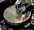
CIS Test
>Business>CIS Test
CIS Test process to check whether the entire chip on the CMOS Image Sensor Wafer is correctly operated through O/S and Function check by using each IC exclusive tester. After the electrical test, defective chips (reject die) can be inked on the chip surface or provided as a test map, so that only the good chip (Good Die) can be assembled during the subsequent A’ssy process. ALT provides optimal testing services by building CIS exclusive facilities capable of high-speed image capture and max. 64 DUT parallel tests.

Probe Test Process

-
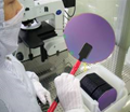
- Wafer (6”, 8”, 12”)
1
-
- Image High & low Power Scope
- Clean Room (10 Class)
2
-
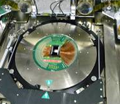
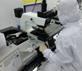
- Electrical Testing
- Program Development
3
-
- Auto Visual Inspection
4
-
- Wafer Reject Dies Inking
- Clean Bake Oven
5
-
- Image High & low Power Scope
- Sampling or All
6
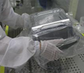
-
- Barcode Labeling
- Packing Machine
7
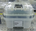
-
- Packing & Sheet Inspection
8
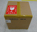
-
- Out box Packing
9